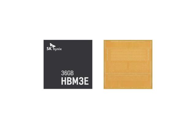
The 36GB chip, designed for artificial intelligence chipsets, features DRAMs that are 40 percent thinner than previous versions, increasing capacity by 50 percent while maintaining the same overall thickness, according to the world's second-largest memory chip maker.
Operating at 9.6 gigabits per second, a single graphics processing unit (GPU) equipped with four of these chips can efficiently process large language models.
SK hynix achieved this by vertically stacking 12 3GB DRAM chips using TSV (Through Silicon Via) technology.
The company improved thermal performance and structural stability through its proprietary advanced mass reflow-molded underfill (MR-MUF) process, which helps control warpage and enhances reliability.
Kim Ju-sun, president of AI Infra at SK Hynix, stated, "We have once again proven our position as a leader in AI memory by pushing the boundaries of technology."
reporter

Candice Kim
candicekim1121@ajupress.com
Copyright ⓒ Aju Press All rights reserved.
View more comments