[Courtesy of KAIST]
SEOUL -- South Korean researchers have developed non-destructive testing equipment that uses near-infrared rays to detect the thickness and the porous structure of silicon wafers. Chipmakers can test the quality of products without having to destroy randomly selected semiconductors during their test process.
In semiconductor production, chips are randomly selected from each manufacturing line to test their quality. Chips are cut into pieces and put under a microscope to test micrometer-thick films and the structure of silicon wafers. If defects are found, production lines will be stopped for extra tests.
In destructive tests, chips are discarded even though they meet quality standards. The cost induced by the loss of tested chips is quite large considering some 250,000 wafers are made annually. Wafers that are micrometer-thin are widely used in pressure sensors, radio transmitters, and other complicated tiny-sized electrical devices.
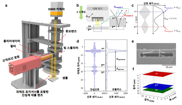
The Korea Advanced Institute of Science & Technology (KAIST) said that its research team has developed a non-destructive testing microscope device that utilizes a near-infrared interference effect. The microscope is capable of testing the film structure of wafers that are less than one micrometer thick.
The research team found that the newly-developed microscope can be used for the testing of silicon-on-insulator type wafers and other semiconductor materials such as germanium. The non-destructive test device can be adopted into a standardized quality management system to be operated in real-time.
"This test equipment differentiates from its predecessors because it uses widely-used infrared light sources in a non-destructive way and it would bring positive effects to our everyday lives by accelerating test speeds thanks to its safe and accurate characteristics," KAIST researcher Lee Jeong-cheol said in a statement on December 19.
Copyright ⓒ Aju Press All rights reserved.


View more comments